
Product Info

LTE Module Series
BG96 Hardware Design
BG96_Hardware_Design 37 / 81
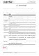
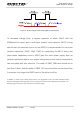
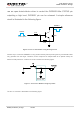
Module
VB AT_RF
VB AT_BB
VB AT
C1
100uF
C6 C7 C8
+
+
C2
100nF
C5
C3
33pF
C4
10pF
D1
TVS
100uF
100nF
33pF
10pF
Figure 5: Star Structure of the Power Supply
3.5.3. Monitor the Power Supply
AT+CBC command can be usedto monitor the VBAT_BB voltage value. For more details, please refer to
document [2].
3.6. Turn on and off Scenarios
3.6.1. Turn on Module Using the PWRKEY Pin
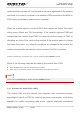
The following table shows the pin definition of PWRKEY.
Table 7: Pin Definition of PWRKEY
When BG96 is in power off mode, it can be turned on to normal mode by
driving the PWRKEY pin to a low level for at least 500ms. It is recommended to
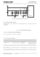
Pin Name Pin No. Description DC Characteristics Comment
PWRKEY 15 Turn on/off the module
Vnorm=0.8V
V
IL
max=0.5V
The output voltage is0.8V
because of thediode drop
in theQualcomm chipset.