
Product Info


LTE Module Series
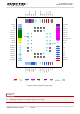
BG96 Hardware Design
BG96_Hardware_Design 27 / 81
Pin Name Pin No. I/O Description
DC
Characteristics
Comment
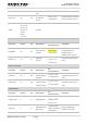
UART3_TXD
27 DO
Transmit data
V
OL
max=0.45V
V
OH
min=1.35V
1.8V power domain.
If unused, keep this pin
open.
UART3_RXD 28 DI Receive data
V
IL
min=-0.3V
V
IL
max=0.6V
V
IH
min=1.2V
V
IH
max=2.0V
1.8V power domain.
If unused, keep this pin
open.
PCM* Interface
Pin Name Pin No. I/O Description
DC
Characteristics
Comment
PCM_CLK* 4 DO
PCMclock
output
V
OL
max=0.45V
V
OH
min=1.35V
1.8V power domain.
If unused, keep this pin
open.
PCM_SYNC* 5 DO
PCMframe
synchronization
output
V
OL
max=0.45V
V
OH
min=1.35V
1.8V power domain.
If unused, keep this pin
open.
PCM_IN* 6 DI
PCMdata input
V
IL
min=-0.3V
V
IL
max=0.6V
V
IH
min=1.2V
V
IH
max=2.0V
1.8V power domain.
If unused, keep this pin
open.
PCM_OUT* 7 DO
PCMdata
output
V
OL
max=0.45V
V
OH
min=1.35V
1.8V power domain.
If unused, keep this pin
open.
I2C* Interface
Pin Name Pin No. I/O Description
DC
Characteristics
Comment
I2C_SCL* 40 OD
I2C serial clock.
Used for
external codec.
External pull-up resistor
is required.
1.8V only.
If unused, keep
this pin open.
I2C_SDA* 41 OD
I2C serial data.
Used for
external codec.
External pull-up resistor
is required.
1.8V only.
If unused, keep this pin
open.