
User's Manual


LTE Module Series
EC21 Hardware Design
EC21_Hardware_Design Confidential / Released 61 / 94
B12 699~716 729~746 MHz
B13 777~787 746~756 MHz
B18 815~830 860~875 MHz
B19 830~845 875~890 MHz
B20 832~862 791~821 MHz
B26 814~849 859~894 MHz
B28 703~748 758~803 MHz
B40 2300~2400 2300~2400 MHz
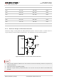
5.1.3. Reference Design of RF Antenna Interface
Areference design of ANT_MAIN and ANT_DIVantenna pads is shown as below. It should reserve a
π-type matching circuit for better RF performance. The capacitors are not mounted by default.
Figure 31: Reference Circuit of RF Antenna Interface
1. Keep a proper distance between the main antenna and the Rx-diversity antenna to improve the
receiving sensitivity.
2. ANT_DIV function is enabledby default.
3. Place the π-type matching components (R1, C1, C2, R2, C3, C4) as close to the antenna as
possible.
NOTES