
User's Manual

LTE Module Series
EC21 Hardware Design
EC21_Hardware_Design Confidential / Released 48 / 94
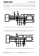
3.13. ADC Function
The module provides two analog-to-digital converters (ADC).AT+QADC=0 command can be used to read
the voltage value on ADC0 pin. AT+QADC=1command can be used to read the voltage value on ADC1
pin. For more details about these AT commands, please refer todocument [2].
In order to improve the accuracy of ADC, the trace of ADC should be surrounded by ground.
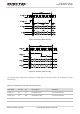
Table 15: Pin Definition of the ADC
Pin Name Pin No. Description
ADC0 45 General purpose analog to digital converter
ADC1 44 General purpose analog to digital converter
The following table describes the characteristic of the ADC function.
Table 16: Characteristic of the ADC
Parameter Min. Typ. Max. Unit
ADC0 Voltage Range 0.3 VBAT_BB V
ADC1 Voltage Range 0.3 VBAT_BB V
ADC Resolution 15 bits
1. ADC input voltage must not exceed VBAT_BB.
2. It is prohibited to supply any voltage to ADC pins when VBAT is removed.
3. It is recommended to use resistor divider circuit for ADC application.
NOTES