
User's Manual

LTE Module Series
EC21 Hardware Design
EC21_Hardware_Design Confidential / Released 42 / 94
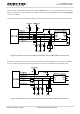
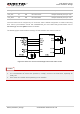
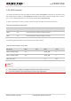
The USB interface is recommended to be reserved for firmware upgrade in your design. The following
figure shows areference circuit of USB interface.
Figure 19: Reference Circuit of USB Application
In order to ensurethe integrity of USB data line signal, components R1, R2, R3 and R4 must be placed
close to the module, and alsothese resistors should be placed close to each other. The extra stubs of
trace must be as short as possible.
In order to ensure the USB interface design corresponding with the USB 2.0 specification, please comply
with the following principles:
It is important to route the USB signal traces as differential pairs with total grounding. The impedance
of USB differential trace is 90ohm.
Do not route signal traces under crystals, oscillators, magnetic devicesorRF signal traces. It is
important to route the USB differential traces in inner-layer with ground shielding onnot only upper
and lower layers but also right and left sides.
Pay attention to the influence of junction capacitance of ESD protection components on USB data
lines. Typically, the capacitance value should be less than 2pF.
Keep the ESD protection components to the USB connector as close as possible.
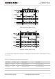
1. EC21 module can only be used as a slave device.
2. “*” means under development.
NOTES