
User's Manual


LTE Module Series
EC21 Hardware Design
EC21_Hardware_Design Confidential / Released 33 / 94
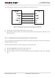
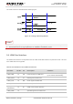
Table 6: VBAT and GND Pins
Pin Name Pin No. Description Min. Typ. Max. Unit
VBAT_RF 57,58
Power supply for module RF
part.
3.3 3.8 4.3 V
VBAT_BB 59,60
Power supply for module
baseband part.
3.3 3.8 4.3 V
GND
8,9,19,22,36,46
, 48,50~54,56,
72, 85~112
Ground - 0 - V
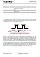
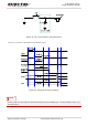
3.6.2. Decrease Voltage Drop
The power supply range of the module is from 3.3Vto4.3V. Please make sure that the input voltage will
never drop below 3.3V. The following figure shows the voltage drop during burst transmission in 2G
network.The voltage drop will be less in 3G and 4G networks.
Figure 7: Power Supply Limits during Burst Transmission
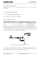
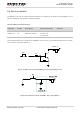
To decrease voltage drop, a bypass capacitor of about 100µF with low ESR should be used, and
amulti-layer ceramic chip (MLCC) capacitorarray should also be used to provide the low ESR. The main
power supply from an external application has to be a single voltage source and can be expanded to two
sub paths with star structure. The width of VBAT_BB trace should be no less than 1mm; andthe width of
VBAT_RF trace should be no less than 2mm.In principle, the longerthe VBAT trace is, the wider it will be.
Three ceramic capacitors (100nF, 33pF, 10pF) are recommended to be applied to the VBAT pins. These
capacitors should be placed close to the VBAT pins. In addition, in order to get a stable power source, it is
suggested that you should use a zener diode of which reverse zener voltage is 5.1V and dissipation
power is more than 0.5W. The following figure shows the star structure of the power supply.