
User's Manual

LTE Module Series
EC21 Hardware Design
EC21_Hardware_Design Confidential / Released 19 / 94
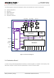
module.
6. Keep all RESERVEDpins and unused pins unconnected.
7. GND pads 85~112 should be connected to ground in the design, and RESERVED pads 73~84should
not be designed in schematic and PCB decal.
8. “
※
” means these interface functions are only supported on Telematics version.
3.3. Pin Description
The following tables show the pin definition of EC21 module.
Table 3: I/O Parameters Definition
Type Description
IO Bidirectional
DI Digital input
DO Digital output
PI Power input
PO Power output
AI Analog input
AO Analog output
OD Open drain
Table 4: Pin Description
Power Supply
Pin Name Pin No. I/O Description DC Characteristics Comment
VBAT_BB 59,60 PI
Power supply for
module baseband
part
Vmax=4.3V
Vmin=3.3V
Vnorm=3.8V
It must be able to provide
sufficient current up to
0.8A.
VBAT_RF 57,58 PI
Power supply for
module RF part
Vmax=4.3V
Vmin=3.3V
Vnorm=3.8V
It must be able to provide
sufficient current up to
1.8A in a burst
transmission.