
User's Manual

LTE Module Series
EC21 Hardware Design
EC21_Hardware_Design Confidential / Released 18 / 94
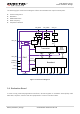
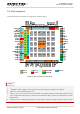
3.2. Pin Assignment
The following figure shows the pin assignment of EC21 module.
Figure 2: Pin Assignment (Top View)
1.
1)
means that these pins cannot be pulled up before startup.
2.
2)
PWRKEY output voltage is 0.8V because of the diode drop in the Qualcomm chipset.
3. Pads 119~126 are SGMII function pins.
4. Pads 37~40, 118, 127 and 129~139 are wireless connectivity interfaces, among which pads 127 and
129~138 are WLAN function pins, and others are Bluetooth (BT) function pins. BT function is under
development.
5. Pads 24~27 are multiplexing pinsused for audio design on EC21 module and BT function on FC20
NOTES