
User's Manual


LTE Module Series
BG96 Hardware Design
BG96_Hardware_Design Confidential / Released 61 / 71
possible and its corresponding reference ground in the opposite layer is as integrated as possible,
meanwhile ensure the two layer ground is connected by amount of ground hole.
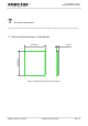
6. Three components consist of PI type matching circuit shown as Figure 6. Place the pad to antenna
as close as possible, as shown in Figure 6. If the distance between SMA and RF PIN is too short to
place the three pin of PI type matching circuit, PI type matching circuit can be changed into L
matching circuit.