
User's Manual


LTE Module Series
BG96 Hardware Design
BG96_Hardware_Design Confidential / Released 60 / 71
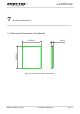
5.3.5. Coplanar WG PCB Layout Example and Guidelines
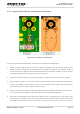
Figure 38: An example of PCB layout
There are 6 guidelines should be taken into account, as marked in the above figure:
1. Control corresponding W and S of 50 ohm coplanar waveguide. Use the common PCB as FR4
medium (dielectric constant is 4.2) and take copper clad of 35 um thickness as an example. Values of
W and S for 50 ohm coplanar WG under different PCB structure is shown as Table 1. Keep in mind to
remind PCB manufacturers to keep the accuracy of W and S.
2. Do not hot sealing the PIN in this position and make it contacted with the ground closely enough.
3. Keep out pouring copper in the surface layer and reduce parasitic effect. The RF trace line should be
as short as possible. It will be better for RF trace line to avoid vertical angle layout. The RF trace
line should be kept 135 degree angle around the corner.
4. Keep a certain distance between signal pad and ground when packaging the device. Refer to Figure
6. If the signal pad is in SMD type, pouring copper on the corresponding signal pad.
5. Ensure the corresponding reference ground of RF trace line is integrated and do not forget to add
more ground via to help RF reflow. The ground and RF trace should be kept at least two times of the
trace width. Guarantee the contact area which is in the same layer with RF trace is as large as