
User's Manual


LTE Module Series
BG96 Hardware Design
BG96_Hardware_Design Confidential / Released 59 / 71
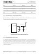
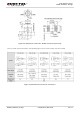
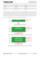
If there are two layers, the TOP layer is the signal layer, and the BOTTOM layer is the reference ground,
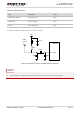
as shown in Figure 3. If there are 4 layers, the reference ground could be the second layer, the third layer
or the fourth layer. If third layer is chosen, the second layer should be kept out and the width of keepout
area should be at least five times of the trace width, as shown in Figure 4. If the fourth layer is chosen,
both the second and third layer should be kept out and the width of keepout area should be at least five
times of the trace width, as shown in Figure 5. Same as 6 or more layers.
Figure 35: Two Layers PCB Layout
Figure 36: Four Layers PCB Layout (Third Layer as Reference Ground)
Figure 37: Four Layers PCB Layout (Fourth Layer as Reference Ground)
1.2mm
0.8mm
0.16mm
1.6mm
0.8mm
0.15mm
2mm
0.8mm
0.14mm