
User's Manual


LTE Module Series
BG96 Hardware Design
BG96_Hardware_Design Confidential / Released 50 / 71
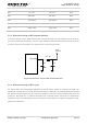
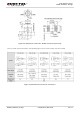
B13
777~787
746~757
MHz
B20
832~862
791~821
MHz
B26
814~848.9
859~893.9
MHz
B28
703~748
758~803
MHz
B39
1880~1920
1880~1920
MHz
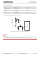
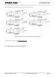
5.1.3. Reference Design of RF Antenna Interface
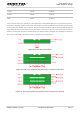
A reference design of ANT_MAIN antenna pad is shown as below. A π-type matching circuit should be
reserved for better RF performance, and the π-type matching components (R1/C1/C2) should be placed
as close the antenna as possible. The capacitors are not mounted by default.
ANT_MAIN
R1 0R
C1
Module
Main
antenna
NM
C2
NM
Figure 24: Reference Circuit of RF Antenna Interface
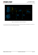
5.1.4. Reference Design of RF Layout
For user’s PCB, the characteristic impedance of all RF traces should be controlled as 50Ω. The
impedance of the RF traces is usually determined by the trace width (W), the materials’ dielectric constant,
the distance between signal layer and reference ground (H), and the clearance between RF trace and
ground (S). Microstrip line or coplanar waveguide line is typically used in RF layout for characteristic
impedance control. The following are reference designs of microstrip line or coplanar waveguide line with
different PCB structures.