
User's Manual

LTE Module Series
BG96 Hardware Design
BG96_Hardware_Design Confidential / Released 42 / 71
I2S_D0*
6
IO
I2S data 0
1.8V power domain
I2S_D1*
7
IO
I2S data 1
1.8V power domain
I2C_SCL
40
OD
I2C serial clock
Require external pull-up to 1.8V
I2C_SDA
41
OD
I2C serial data
Require external pull-up to 1.8V
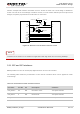
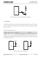
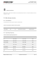
The following figure shows a reference design of I2S* and I2C interfaces with an external codec IC.
I2S_D0
I2S_WCLK
I2S_BCLK
I2S_MCLK
I2C_SCL
I2C_SDA
Module
1.8V
4.7K
4.7K
MCLK
BCLK
WCLK
ADC
SCL
SDA
BIAS
MICBIAS
INP
INN
LOUTP
LOUTN
Codec
I2S_D1
DAC
Figure 20: Reference Circuit of I2S Application with Audio Codec
“*” means under development.
3.12. SPI* Interface
BG96 provides one Serial Peripheral Interface (SPI) digital interface* which is multiplexed from UART3
(default configuration).
The following table shows the pin definition of SPI* interface which can be used to transfer data.
NOTE