
User's Manual

LTE Module Series
BG96 Hardware Design
BG96_Hardware_Design Confidential / Released 41 / 71
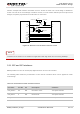
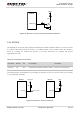
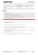
Another example with transistor translation circuit is shown as below. The circuit design of dotted line
section can refer to the circuit design of solid line section, in terms of both module input and output circuit
designs, but please pay attention to the direction of connection.
MCU/ARM
TXD
RXD
VDD_EXT
10K
VCC_MCU
4.7K
10K
VDD_EXT
TXD
RXD
RTS
CTS
DTR
RI
RTS
CTS
GND
GPIO DCD
Module
GPIO
EINT
VDD_EXT
4.7K
GND
1nF
1nF
Figure 19: Reference Circuit with Transistor Circuit
Transistor circuit solution is not suitable for applications with high baud rates exceeding 460Kbps.
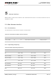
3.11. I2S* and I2C Interfaces
BG96 provides one Inter-IC Sound (I2S) digital interface* and one I2C interface.
The following table shows the pin definition of I2S* and I2C interfaces which can be applied on audio
codec design.
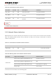
Table 15: Pin Definition of I2S* and I2C Interfaces
Pin Name
Pin No.
I/O
Description
Comment
I2S_MCLK*
63
DO
I2S master clock
1.8V power domain.
I2S_BCLK*
4
DO
I2S bit clock
1.8V power domain
I2S_WCLK*
5
DO
I2S data frame clock
1.8V power domain
NOTE