
User's Manual

LTE Module Series
BG96 Hardware Design
BG96_Hardware_Design Confidential / Released 24 / 71
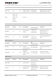
ANT_MAIN
60
IO
Main antenna
interface
50Ω impedance
ANT_GNSS
49
AI
GNSS antenna
interface
50Ω impedance
If unused, keep it open.
Other Pins
Pin Name
Pin No.
I/O
Description
DC
Characteristics
Comment
PSM_IND*
1
DO
Power saving
mode indicator
V
IL
min=-0.3V
V
IL
max=0.6V
V
IH
min=1.2V
V
IH
max=2.0V
1.8V power domain.
If unused, keep it open.
W_DISABLE#
18
DI
Airplane mode
control
V
IL
min=-0.3V
V
IL
max=0.6V
V
IH
min=1.2V
V
IH
max=2.0V
1.8V power domain.
Pull-up by default.
In low voltage level, the
module can enter into
airplane mode.
If unused, keep it open.
AP_READY*
19
DI
Application
processor sleep
state detection
V
IL
min=-0.3V
V
IL
max=0.6V
V
IH
min=1.2V
V
IH
max=2.0V
1.8V power domain.
If unused, keep it open.
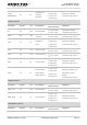
USB_BOOT
75
DI
Force the
module to boot
from USB port
V
IL
min=-0.3V
V
IL
max=0.6V
V
IH
min=1.2V
V
IH
max=2.0V
1.8V power domain.
If unused, keep it open.
GPIO*
64
IO
General-
purpose input/
output interface
V
IL
min=-0.3V
V
IL
max=0.6V
V
IH
min=1.2V
V
IH
max=2.0V
1.8V power domain.
If unused, keep it open.
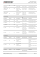
ADC Interface
Pin Name
Pin No.
I/O
Description
DC
Characteristics
Comment
ADC1
2
AI
General
purpose analog
to digital
converter
interface
Voltage range:
0.3V to VBAT_BB
If unused, keep it open.
ADC0
24
AI
General
purpose analog
to digital
converter
interface
Voltage range:
0.3V to VBAT_BB
If unused, keep it open.