
User's Manual

LTE Module Series
BG96 Hardware Design
BG96_Hardware_Design Confidential / Released 19 / 71
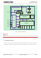
1. Keep all RESERVED pins and unused pins unconnected.
2. GND pads should be connected to ground in the design.
3.
1)
PWRKEY output voltage is 0.8V because of the diode drop in the Qualcomm chipset.
4. “*” means under development.
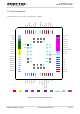
3.2. Pin Description
The following tables show the pin definition and description of BG96.
Table 3: Definition of I/O Parameters
Type
Description
IO
Bidirectional
DI
Digital input
DO
Digital output
PI
Power input
PO
Power output
AI
Analog input
AO
Analog output
OD
Open drain
Table 4: Pin Description
Power Supply
Pin Name
Pin No.
I/O
Description
DC
Characteristics
Comment
VBAT_BB
32, 33
PI
Power supply
for module
baseband part
Vmax=4.3V
Vmin=3.3V
Vnorm=3.8V
VBAT_RF
52, 53
PI
Power supply
for module RF
Vmax=4.3V
Vmin=3.3V
NOTES