
User's Manual


LTE Module Series
BG96-NA Hardware Design
BG96-NA_Hardware_Design Confidential / Released 17 / 64
3.3. Pin Description
The following tables show the pin definition and description of BG96-NA.
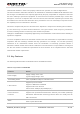
Table 3: I/O Parameters Definition
Type
Description
IO
Bidirectional
DI
Digital input
DO
Digital output
PI
Power input
PO
Power output
AI
Analog input
AO
Analog output
OD
Open drain
Table 4: Pin Description
Power Supply
Pin Name
Pin No.
I/O
Description
DC
Characteristics
Comment
VBAT_BB
32, 33
PI
Power supply
for module
baseband part.
Vmax=4.3V
Vmin=3.3V
Vnorm=3.8V
VBAT_RF
52, 53
PI
Power supply
for module RF
part.
Vmax=4.3V
Vmin=3.3V
Vnorm=3.8V
VDD_EXT
29
PO
Provide 1.8V for
external circuit.
Vnorm=1.8V
I
O
max=50mA
Power supply for external
GPIO’s pull up circuits.
GND
3, 31, 48,
50, 54, 55,
58, 59, 61,
62, 67~74,
79~82,
89~91,
100~102
Ground