
User's Manual


LTE Module Series
BG96-NA Hardware Design
BG96-NA_Hardware_Design Confidential / Released 13 / 64
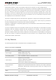
2.4. Functional Diagram
The following figure shows a block diagram of BG96-NA and illustrates the major functional parts.
Power management
Baseband
DDR+NAND flash
Radio frequency
Peripheral interfaces
Baseband
PMIC
Transceiver
NAND
DDR2
SDRAM
PA
Switch
Filter
ANT_MAIN ANT_GNSS
VBAT_BB
VBAT_RF
PWRKEY
VDD_EXT
USB USIM UARTI2C
RESET_N
19.2M
XO
STATUS
GPIOs
Control
IQ Control
LNA
Tx
PRx
GNSS
Figure 1: Functional Diagram
“*” means under development.
NOTE