
User's Manual

FC20-N Series Hardware Design
FC20-N_Series_Hardware_Design Confidential / Released 24 /
47
Table 10: Pin Definition of DBG_TXD Interface
Pin Name
Pin No.
I/O
Description
Comment
DBG_TXD
4
DO
Software debugging
If unused, keep this pin
open.
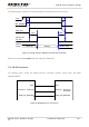
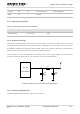
3.7.2. 32KHz_IN Interface
The 32KHz clock is used in low power mode such as IEEE power saving mode and sleep mode. It serves
as a timer to determine when to wake up FC20 series module to receive beacons in various power saving
schemes, and to maintain basic logic operations when in sleep mode. The sleep clock signal is
transferred from EC20 R2.0/EC21/EC25 module.
Table 11: Pin Definition of 32KHz_IN Interface
Pin Name
Pin No.
I/O
Description
Comment
32KHz_IN
19
DI
Low power.
External 32.768KHz
clock input is required
in sleep mode.
If unused, keep this pin
open.
3.8. Antenna Interface
The pin 30 is the RF antenna pad. And the RF interface has an impedance of 50Ω.
3.8.1. Pin Definition of the RF Antenna
Table 12: Pin Definition of the RF Antenna
Pin Name
Pin No.
I/O
Description
Comment
GND
28
Ground
GND
29
Ground