
User's Manual

FC20-N Series Hardware Design
FC20-N_Series_Hardware_Design Confidential / Released 22 /
47
1.8V.
SDIO_D1
24
IO
SDIO data pin bit 1
1.8V power domain
SDIO_D0
25
IO
SDIO data pin bit 0
1.8V power domain
SDIO_CLK
26
DI
SDIO clock
1.8V power domain
SDIO_CMD
27
IO
SDIO command
1.8V power domain
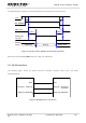
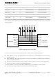
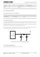
The following figure shows the SDIO interface connection between FC20 series and EC20
R2.0/EC21/EC25.
SDIO_CLK
SDIO_CMD
SDIO_D0
SDIO_D1
SDIO_D2
SDIO_D3
EC20 R2.0/
EC21/EC25
FC20 Series
SD1_D0
SD1_D1
SD1_D2
SD1_D3
SD1_CLK
SD1_CMD
10K
NM_10K
VIO
VIO
VIO
VIO VIO
VIO
NM_10K
NM_10K
NM_10K
NM_10K
NM_10nF
Figure 6: SDIO Interface Connection
In order to ensure the performance of SDIO, please comply with the following principles:
SDIO signals are very high-speed signals. Please prevent crosstalk between them and other
sensitive signals.
Keep SDIO traces as parallel as possible in the same layer. Make sure SDIO lines are guarded by
ground vias and not crossed.
Do not route SDIO signal traces under crystals, oscillators, magnetic devices and RF signal traces.
The pull-up resistor on SDIO_D2 line must be mounted.
Keep SDIO traces as short as possible with equal length, and impedance control as 50Ω.
The spacing to all other signals is greater than 2 times of the line width.