
User's Manual

Wi-Fi&BT Module Series
FC20 Series Hardware Design
FC20_Series_Hardware_Design Confidential / Released 25 / 47
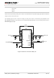
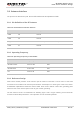
Table 10: Pin Definition of PCM Interface
Pin Name
Pin No.
I/O
Description
Comment
PCM_IN
13
DI
PCM data input
1.8V power domain
PCM_SYNC
14
IO
PCM data frame
sync signal
1.8V power domain
PCM_CLK
15
IO
PCM data bit clock
1.8V power domain
PCM_OUT
16
DO
PCM data output
1.8V power domain
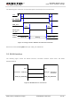
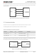
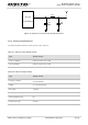
The following figure shows the reference design for PCM interface.
PCM_IN
PCM_OUT
PCM_SYNC
PCM_CLK
FC20
PCM_CLK
PCM_SYNC
PCM_IN
PCM_OUT
EC20 R2.0/
EC21/EC25
Figure 8: Reference Design for PCM Interface
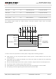
3.6.3. UART Interface
The following table shows the pin definition of UART interface.
Table 11: Pin Definition of UART Interface
Pin Name
Pin No.
I/O
Description
Comment
BT_UART_RTS
7
DO
Request to send
1.8V power domain
BT_UART_CTS
8
DI
Clear to send
1.8V power domain
BT_UART_TXD
17
DO
Bluetooth transmits data
1.8V power domain
BT_UART_RXD
18
DI
Bluetooth receives data
1.8V power domain