
User's Manual


GSM/GPRS/GNSS Module Series
MC60 Hardware Design
MC60_Hardware_Design Confidential / Released 64 / 99
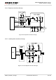
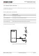
Figure 37: Reference Circuit for SIM2 Interface with a 6-pin SIM Card Holder
For more information of SIM card holder, you can visit http://www.amphenol.com/ and
http://www.molex.com/.
In order to enhance the reliability and availability of the SIM card in application, please conform to the
following criteria in the SIM circuit design:
Keep layout of SIM card as close to the module as possible. Assure the trace length is less than
200mm.
Keep SIM card signal away from RF and VBAT alignment.
Assure the ground between module and SIM cassette short and wide. Keep the width of ground no
less than 0.5mm to maintain the same electric potential. The decouple capacitor of SIM_VDD is less
than 1uF and must be near to SIM cassette.
To avoid cross talk between SIM_DATA and SIM_CLK, keep them away from each other and shield
them with surrounded ground.
In order to offer good ESD protection, it is recommended to add a TVS diode array. For more
information of TVS diode, please visit http://www.onsemi.com/. The most important rule is to place
the ESD protection device close to the SIM card socket and make sure the nets being protected will
go through the ESD device first and then lead to module. The 22Ω resistors should be connected in
series between the module and the SIM card so as to suppress the EMI spurious transmission and
enhance the ESD protection. Please note that the SIM peripheral circuit should be close to the SIM
card socket.
Place the RF bypass capacitors (33pF) close to the SIM card on all signals lines to improve EMI
suppression performance.