
User's Manual

GSM/GPRS/GNSS Module Series
MC60 Hardware Design
MC60_Hardware_Design Confidential / Released 29 / 99
3.3.2.2. Decrease Supply Voltage Drop for GNSS Part
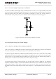
The same as VBAT, power supply range of GNSS part is from 2.8 to 4.3V. Typical GNSS_VCC peak
current is 40mA during GNSS acquisition after power up. So it is important to supply sufficient current and
make the power clean and stable. The decouple combination of 10uF and 100nF capacitor is
recommended nearby GNSS_VCC pin. A reference circuit is illustrated in the following figure.
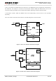
Figure 7: Reference Circuit for the GNSS_VCC Input
3.3.3. Reference Design for Power Supply
3.3.3.1. Reference Design for Power Supply of GSM Part
In all-in-one solution, the GSM part controls the power supply of the GNSS part. Therefore, the GSM part
share the same power circuit design in both all-in-one and stand-alone solutions.
The power supply of GSM part is capable of providing sufficient current up to 2A at least. If the voltage
drop between the input and output is not too high, it is suggested to use a LDO as the module’s power
supply. If there is a big voltage difference between the input source and the desired output (VBAT), a
switcher power converter is recommended to be used as the power supply.
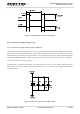
The following figure shows a reference design for +5V input power source for GSM part. The designed
output for the power supply is 4.0V and the maximum load current is 3A. In addition, in order to get a
stable output voltage, a zener diode is placed close to the pins of VBAT. As to the zener diode, it is
suggested to use a zener diode whose reverse zener voltage is 5.1V and dissipation power is more than 1
Watt.