
User's Manual

GSM/GPRS/GNSS Module Series
MC60 Hardware Design
MC60_Hardware_Design Confidential / Released 21 / 99
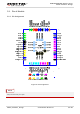
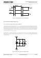
3.1.2. Pin Description
Table 5: I/O Parameters Definition
Type Description
IO Bidirectional input/output
DI Digital input
DO Digital output
PI Power input
PO Power output
AI Analog input
AO Analog output
Table 6: Pin Description
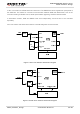
Power Supply
PIN Name PIN No. I/O Description DC Characteristics Comment
VBAT 50, 51 PI
Power supply of
GSM/GPRS part:
VBAT=3.3V~4.6V
V
I
max=4.6V
V
I
min=3.3V
V
I
norm=4.0V
It must be able to
provide sufficient
current up to 1.6A
in a transmitting
burst.
GNSS_
VCC
26 PI
Power supply of GNSS
part:
VBAT=2.8V~4.3V
V
I
max=4.3V
V
I
min=2.8V
V
I
norm=3.3V
Assure load
current no less
than 150mA.
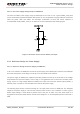
VRTC 52 IO
Power supply for GNSS’s
backup domain
Charging for backup
battery or golden
capacitor when the VBAT
is applied.
VImax=3.3V
VImin=1.5V
VInorm=2.8V
VOmax=3V
VOmin=2V
VOnorm=2.8V
IOmax=2mA
Iin≈14uA
Refer to Section
3.3.5
VDD_
EXT
43 PO
Supply 2.8V voltage for
external circuit.
V
O
max=2.9V
V
O
min=2.7V
V
O
norm=2.8V
I
O
max=20mA
1. If unused, keep
this pin open.
2. Recommend
adding a