
User's Manual
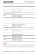

GSM/GPRS/GNSS Module Series
MC20 Hardware Design
MC20_Hardware_Design Confidential / Released 70 / 95
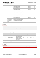
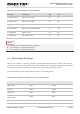
4.2.2. Active Antenna
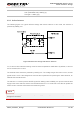
The following figure is a typical reference design with active antenna. In this mode, the antenna is
powered by GNSS_VCC.
Figure 39: Reference Design with Active Antenna
C1, R1 and C2 are reserved matching circuit for antenna impedance modification. By default, C1 and C2
are not mounted; R1 is 0 ohm.
The external active antenna is powered by GNSS_VCC. The voltage ranges from 2.8V to 4.3V, and the
typical value is 3.3V. If the voltage does not meet the requirements for powering the active antenna, an
external LDO should be used.
The inductor L1 is used to prevent the RF signal from leaking into the GNSS_VCC pin and route the bias
supply to the active antenna, and the recommended value of L1 is no less than 47nH. R2 can protect the
whole circuit in case the active antenna is shorted to ground.
In all-in-one solution, please note that the power supply of GNSS_VCC is controlled by the GSM part
through AT command.
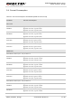
Gain (antenna): >-2dBi
Gain (embedded LNA): 20dB (Typ.)
Total gain: >18dBi (Typ.)
NOTE