
User's Manual

GSM/GPRS/GNSS Module Series
MC20 Hardware Design
MC20_Hardware_Design Confidential / Released 58 / 95
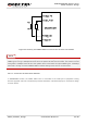
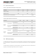
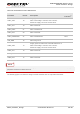
Table 19: Pin Definition of the SIM Interface
1)
If several interfaces share the same I/O pin, to avoid conflict between these alternate functions, only one
peripheral should be enabled at a time.
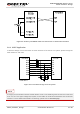
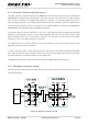
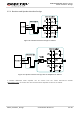
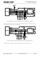
The following figure is a reference design for SIM1 interface with an 8-pin SIM card holder.
Pin Name Pin No. Description
Alternate
Function
1)
SIM1_VDD 18
Supply power for SIM card. Automatic detection of
SIM1 card voltage. 3.0V±5% and 1.8V±5%.
Maximum supply current is around 10mA.
SIM1_CLK 19 SIM1 card clock.
SIM1_DATA 21 SIM1 card data I/O.
SIM1_RST 20 SIM1 card reset.
SIM1_PRESENCE 37 SIM1 card detection. DTR
SIM_GND 16 SIM card ground.
SIM2_VDD 13
Supply power for SIM card. Automatic detection of
SIM2 card voltage. 3.0V±5% and 1.8V±5%.
Maximum supply current is around 10mA.
SIM2_CLK 10 SIM2 card clock.
SIM2_DATA 11 SIM2 card data I/O.
SIM2_RST 12 SIM2 card reset.
NOTE