
User's Manual


GSM/GPRS/GNSS Module Series
MC20 Hardware Design
MC20_Hardware_Design Confidential / Released 30 / 95
3.3.3. Reference Design for Power Supply
3.3.3.1. Reference Design for Power Supply of GSM Part
The power supply of GSM part is capable of providing sufficient current up to 2A at least. If the voltage
drop between the input and output is not too high, it is suggested to use a LDO as the GSM part’s power
supply. If there is a big voltage difference between the input source and the desired output (VBAT), a
switcher power converter is recommended to be used as the power supply.
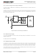
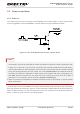
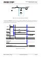
The following figure shows a reference design for +5V input power source for GSM part. The designed
output for the power supply is 4.0V and the maximum load current is 3A. In addition, in order to get a
stable output voltage, a zener diode is placed close to the pins of VBAT. As to the zener diode, it is
suggested to use a zener diode whose reverse zener voltage is 5.1V and dissipation power is more than 1
Watt.
Figure 8: Reference Circuit for Power Supply of the GSM Part
It is suggested to control the module’s main power supply (VBAT) via LDO enable pin to restart the
module when the module becomes abnormal. Power switch circuit like P-channel MOSFET switch circuit
can also be used to control VBAT.
NOTE