
User's Manual
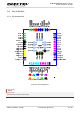

GSM/GPRS/GNSS Module Series
MC20 Hardware Design
MC20_Hardware_Design Confidential / Released 23 / 95
RXD 33 DI Receive data
V
IL
max=
0.25×VDD_EXT
V
IH
min=
0.75×VDD_EXT
V
IH
max=
VDD_EXT+0.2
V
OH
min=
0.85×VDD_EXT
V
OL
max=
0.15×VDD_EXT
and GND are
used for
communication, it
is recommended
to keep all other
pins open.
DTR 37 DI Data terminal ready
RI 35 DO Ring indication
DCD 36 DO Data carrier detection
CTS 38 DO Clear to send
RTS 39 DI Request to send
Debug Port
PIN Name PIN No. I/O Description DC Characteristics Comment
DBG_
TXD
29 DO Transmit data
The same as UART
port
If unused, keep
these pins open.
DBG_
RXD
30 DI Receive data
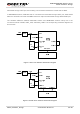
Auxiliary UART Port
PIN Name PIN No. I/O Description DC Characteristics Comment
TXD_
AUX
25 DO Transmit data
The same as UART
port
Refer to Chapter
3.6.3
RXD_
AUX
24 DI Receive data
GNSS UART Port
PIN Name PIN No. I/O Description DC Characteristics Comment
GNSS_
TXD
22 DO Transmit data
V
OL
max=0.42V
V
OH
min=2.4V
V
OH
nom=2.8V
V
IL
min=-0.3V
V
IL
max=0.7V
V
IH
min=2.1V
V
IH
max=3.1V
Refer to Chapter
3.6.3
GNSS_
RXD
23 DI Receive data
SIM Interface
PIN Name PIN No. I/O Description DC Characteristics Comment
SIM1_ VDD
SIM2_ VDD
18
13
PO
Power supply for SIM
card
The voltage can be
selected by software
automatically. Either
1.8V or 3.0V.
All signals of SIM
interface should
be protected
against ESD with
a TVS diode
array.
SIM1_ CLK
SIM2_ CLK
19
10
DO SIM clock
V
OL
max=
0.15×SIM_VDD