
User's Manual


LTE Module Series
EC25-V User Manual
EC25-V_User_Manual Confidential / Released 39 /
69
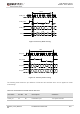
PCM_CLK
PCM_SYNC
PCM_OUT
MSB
LSB
MSB
125us
1 2 256255
PCM_IN
MSB
LSBMSB
Figure 22: Primary Mode Timing
PCM_CLK
PCM_SYNC
PCM_OUT
MSB
LSB
PCM_IN
125us
MSB
1 2 1615
LSB
Figure 23: Auxiliary Mode Timing
The following table shows the pin definition of PCM and I2C interface which can be applied on audio
codec design.
Table 14: Pin Definition of PCM and I2C Interface
Pin Name
Pin No.
I/O
Description
Comment
PCM_IN
24
DI
PCM data input
1.8V power domain