
User's Manual

LTE Module
EC20 Hardware Design
EC20_Hardware_Design Confidential / Released 42 / 83
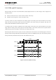
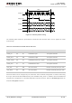
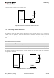
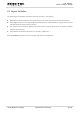
The following figure shows the reference design of PCM interface with external codec IC.
PCM_IN
PCM_OUT
PCM_SYNC
PCM_CLK
I2C_SCL
I2C_SDA
Module
1.8V
4.7K
4.7K
BCLK
LRCK
DAC
ADC
SCL
SDA
BIAS
MICBIAS
INP
INN
LOUTP
LOUTN
ALC5616
Figure 24: Reference Circuit of PCM Application with Audio Codec
1. It is recommended to reserved RC (R=22ohm, C=22pF) circuit on the PCM lines, especially for
PCM_CLK.
2. EC20 works as a master device pertaining to I2C interface.
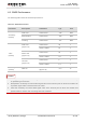
3.13. ADC Function
The module provides two analog-to-digital converters (ADC) to digitize the analog signal to 15-bit digital
data such as battery voltage, temperature and so on. Using AT command AT+QADC=0 can read the
voltage value on ADC0 pin. Using AT command AT+QADC=1 can read the voltage value on ADC1 pin.
For more details of these AT commands, please refer to document [2].
In order to improve the accuracy of ADC, the trace of ADC should be surrounded by ground.
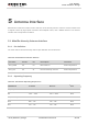
Table 15: Pin Definition of the ADC
Pin Name
Pin No.
Description
ADC0
45
General purpose analog to digital converter
ADC1
44
General purpose analog to digital converter
NOTES