
User's Manual

LTE Module
EC20 Hardware Design
EC20_Hardware_Design Confidential / Released 41 / 83
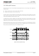
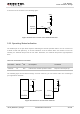
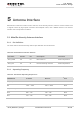
PCM_CLK
PCM_SYNC
PCM_OUT
MSB
LSB
PCM_IN
125us
MSB
1 2 1615
LSB
Figure 23: Auxiliary Mode Timing
The following table shows the pin definition of PCM and I2C interface which can be applied on audio
codec design.
Table 14: Pin Definition of PCM and I2C Interface
Pin Name
Pin No.
I/O
Description
Comment
PCM_IN
24
DI
PCM data input
1.8V power domain
PCM_OUT
25
DO
PCM data output
1.8V power domain
PCM_SYNC
26
IO
PCM data frame sync signal
1.8V power domain
PCM_CLK
27
IO
PCM data bit clock
1.8V power domain
I2C_SCL
41
OD
I2C serial clock
Require external pull-up to 1.8V
I2C_SDA
42
OD
I2C serial data
Require external pull-up to 1.8V
Clock and mode can be configured by AT command, and the default configuration is master mode using
short sync data format with 2048kHz PCM_CLK and 8kHz PCM_SYNC. In addition, EC20’s firmware has
integrated the configuration on ALC5616 application with I2C interface. Refer to document [2] about the
command AT+QDAI for details.