
User's Manual

LTE Module
EC20 Hardware Design
EC20_Hardware_Design Confidential / Released 39 / 83
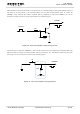
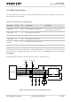
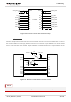
VCCA VCCB
OE
A1
A2
A3
A4
A5
A6
A7
A8
GND
B1
B2
B3
B4
B5
B6
B7
B8
VDD_EXT
RI
DCD
RTS
RXD
DTR
CTS
TXD
51K
51K
0.1uF
0.1uF
RI_MCU
DCD_MCU
RTS_MCU
RXD_MCU
DTR_MCU
CTS_MCU
TXD_MCU
VDD_MCU
Translator
Figure 20: Reference Circuit with Translator Chip
Please visit http://www.ti.com for more information.
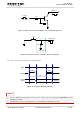
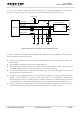
Another example with transistor translation circuit is shown as below. The circuit of dotted line can refer to
the circuit of solid line. Please pay attention to direction of connection. Input dotted line of module should
refer to input solid line of the module. Output dotted line of module should refer to output solid line of the
module.
MCU/ARM
/TXD
/RXD
VDD_EXT
10K
VCC_MCU
4.7K
10K
VDD_EXT
TXD
RXD
RTS
CTS
DTR
RI
/RTS
/CTS
GND
GPIO DCD
Module
GPIO
EINT
VDD_EXT
4.7K
GND
1nF
1nF
Figure 21: Reference Circuit with Transistor Circuit
Transistor circuit solution is not suitable for high baud rate which is more than 460Kbps.
NOTE