
User's Manual

LTE Module
EC20 Hardware Design
EC20_Hardware_Design Confidential / Released 28 / 83
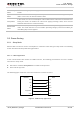
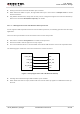
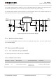
VBAT
Transmit
burst
Transmit
burst
Min.3.3V
Ripple
Drop
Figure 7: Power Supply Limits during Transmit Burst
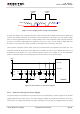
To decrease voltage drop, a bypass capacitor of about 100µF with low ESR should be used. Multi-layer
ceramic chip (MLCC) capacitor can provide the best combination of low ESR. The main power supply
from an external application has to be a single voltage source and expanded to two sub paths with star
structure. The width of VBAT_BB trace should be no less than 1mm, and the width of VBAT_RF trace
should be no less than 2mm, and the principle of the VBAT trace is the longer, the wider.
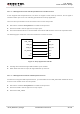
Three ceramic capacitors (100nF, 33pF, 10pF) are recommended to be applied to the VBAT pins. The
capacitors should be placed close to the VBAT pins. In addition, in order to get a stable power source, it is
suggested that you should use a zener diode of which reverse zener voltage is 5.1V and dissipation
power is more than 0.5W. The following figure shows star structure of the power supply.
Module
VBAT_RF
VBAT_BB
VBAT
C1
100uF
C6
100nF
C7
33pF
C8
10pF
+
+
C2
100nF
C5
100uF
C3
33pF
C4
10pF
D1
5.1V
Figure 8: Star Structure of the Power Supply
3.6.3. Reference Design for Power Supply
The power design for the module is very important, since the performance of power supply for the module
largely depends on the power source. The power supply is capable of providing the sufficient current up to
2A at least. If the voltage drop between the input and output is not too high, it is suggested that you should