
User's Manual
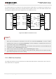
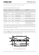
Table Of Contents
- About the Document
- Contents
- Table Index
- Figure Index
- 1 Introduction
- 2 Product Concept
- 3 Application Interface
- 3.1. General Description
- 3.2. Pin Assignment
- 3.3. Pin Description
- 3.4. Operating Modes
- 3.5. Power Saving
- 3.6. Power Supply
- 3.7. Turn on and off Scenarios
- 3.8. Reset the Module
- 3.9. RTC Interface
- 3.10. UART Interface
- 3.11. USIM Card Interface
- 3.12. USB Interface
- 3.13. PCM and I2C Interface
- 3.14. Network Status Indication
- 3.15. Operating Status Indication
- 4 Antenna Interface
- 5 Electrical, Reliability and Radio Characteristics
- 6 Mechanical Dimensions
- 7 Storage and Manufacturing
- 8 Appendix A Reference
- 9 Appendix B GPRS Coding Scheme
- 10 Appendix C GPRS Multi-slot Class
- 11 Appendix D EDGE Modulation and Coding Scheme

UMTS/HSPA Module Series
UG96 Hardware Design
UG96_Hardware_Design Confidential / Released 45 / 75
The following table shows the pin definition of PCM and I2C interface.
Table 14: Pin Definition of PCM and I2C Interface
Pin Name
Pin No. I/O
Description
Comment
PCM_CLK
4
DO
PCM data bit clock
1.8V power domain
PCM_SYNC
5
DO
PCM data frame sync signal
1.8V power domain
PCM_IN
6
DI
PCM data input
1.8V power domain
PCM_OUT
7
DO
PCM data output
1.8V power domain
I2C_SCL
40
OD
I2C serial clock
Require external pull-up resistor.
I2C_SDA
41
OD
I2C serial data
Require external pull-up resistor.
CLK_OUT
25
DO
Clock output
Provide a digital clock output for
an external audio codec.
If unused, keep this pin open.
In PCM audio format the MSB of the channel included in the frame (PCM_SYNC) is clocked on the
second CLK falling edge after the PCM_SYNC pulse rising edge. The period of the PCM_SYNC signal
(frame) lasts for Data word bit +1 clock pulses.
UG96’s firmware has integrated the configurations on NAU8814 /ALC5616/MAX9860 application with I2C
interface. AT+ADQC command is used to configure the external codec chip linked with PCM interface,
and refer to document [1] for more details. Data bit is 32 bit and the sampling rate is 8 KHz. The following
figure shows the timing of the application with ALC5616 codec.
PCM_CLK
PCM_SYNC
PCM_IN/OUT
32
1 0
31
Sampling freq. = 8 KHz
32-bit data word
BCLK = 264 KHz
33
MSB
Figure 27: PCM Master Mode Timing