
User's Manual
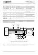
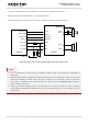
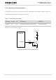
Table Of Contents
- About the Document
- Contents
- Table Index
- Figure Index
- 1 Introduction
- 2 Product Concept
- 3 Application Interface
- 3.1. General Description
- 3.2. Pin Assignment
- 3.3. Pin Description
- 3.4. Operating Modes
- 3.5. Power Saving
- 3.6. Power Supply
- 3.7. Turn on and off Scenarios
- 3.8. Reset the Module
- 3.9. RTC Interface
- 3.10. UART Interface
- 3.11. USIM Card Interface
- 3.12. USB Interface
- 3.13. PCM and I2C Interface
- 3.14. Network Status Indication
- 3.15. Operating Status Indication
- 4 Antenna Interface
- 5 Electrical, Reliability and Radio Characteristics
- 6 Mechanical Dimensions
- 7 Storage and Manufacturing
- 8 Appendix A Reference
- 9 Appendix B GPRS Coding Scheme
- 10 Appendix C GPRS Multi-slot Class
- 11 Appendix D EDGE Modulation and Coding Scheme

UMTS/HSPA Module Series
UG96 Hardware Design
UG96_Hardware_Design Confidential / Released 44 / 75
Keep the ESD components as close as possible to the USB connector.
It is suggested that reserve RC circuit near USB connector for debug.
The USB interface is recommended to be reserved for firmware upgrade in your design. The following
figure shows the recommended test points.
Module
USB_DM
USB_DP
VBAT_BB
USB_VBUS
PWRKEY
GND
VBAT_RF
USB_DM
USB_DP
VBAT
USB_VBUS
PWRKEY
GND
Connector
Figure 26: Test Points of Firmware Upgrade
1. UG96 module can only be used as a slave device.
2. It is suggested that you should set USB_DP, USB_DM and USB_VBUS pins as test points and then
place these test points on the DTE for debug.
3. USB interface supports software debug and firmware upgrade by default.
3.13. PCM and I2C Interface
UG96 provides one Pulse Code Modulation (PCM) digital interface for audio design, which supports the
following features:
Supports 8, 16, 32 bit mode with short frame synchronization, the PCM support 8 bit mode by default.
The PCM codec default configuration is AT+QDAC=1. Refer to document [1] for more details.
Supports master mode.
Supports audio sample rate 8 kHz.
NOTES