
User's Manual
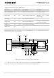
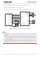
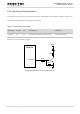
Table Of Contents
- About the Document
- Contents
- Table Index
- Figure Index
- 1 Introduction
- 2 Product Concept
- 3 Application Interface
- 3.1. General Description
- 3.2. Pin Assignment
- 3.3. Pin Description
- 3.4. Operating Modes
- 3.5. Power Saving
- 3.6. Power Supply
- 3.7. Turn on and off Scenarios
- 3.8. Reset the Module
- 3.9. RTC Interface
- 3.10. UART Interface
- 3.11. USIM Card Interface
- 3.12. USB Interface
- 3.13. PCM and I2C Interface
- 3.14. Network Status Indication
- 3.15. Operating Status Indication
- 4 Antenna Interface
- 5 Electrical, Reliability and Radio Characteristics
- 6 Mechanical Dimensions
- 7 Storage and Manufacturing
- 8 Appendix A Reference
- 9 Appendix B GPRS Coding Scheme
- 10 Appendix C GPRS Multi-slot Class
- 11 Appendix D EDGE Modulation and Coding Scheme

UMTS/HSPA Module Series
UG96 Hardware Design
UG96_Hardware_Design Confidential / Released 43 / 75
The following table shows the pin definition of USB interface.
Table 13: USB Pin Description
Pin Name
Pin No. I/O
Description
Comment
USB_DP
9
IO
USB differential data bus (positive).
Require differential
impedance of 90Ω.
USB_DM
10
IO
USB differential data bus (minus).
Require differential
impedance of 90Ω.
USB_VBUS
8
PI
Used for detecting the USB interface
connected.
2.5~5.25V.
Typical 5.0V.
More details about the USB 2.0 specifications, please visit http://www.usb.org/home.
The following figure shows the reference circuit of USB interface.
Module
USB_VBUS
USB_DP
USB_DM
GND
USB connector
Close to USB connector
Differential layout
USB_VBUS
USB_DP
USB_DM
GND
NM_2pF
ESD
NM
NM
Rs
Rs
Figure 25: Reference Circuit of USB Application
In order to ensure the USB interface design corresponding with the USB 2.0 specification, please comply
with the following principles:
It is important to route the USB signal traces as differential pairs with total grounding. The impedance
of USB differential trace is 90ohm.
Pay attention to the influence of junction capacitance of ESD component on USB data lines. Typically,
the capacitance value should be less than 2pF.
Do not route signal traces under crystals, oscillators, magnetic devices and RF signal traces. It is
important to route the USB differential traces in inner-layer with ground shielding not only upper and
lower layer but also right and left side.