
User's Manual
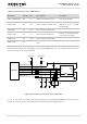
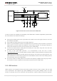
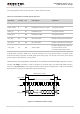
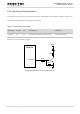
Table Of Contents
- About the Document
- Contents
- Table Index
- Figure Index
- 1 Introduction
- 2 Product Concept
- 3 Application Interface
- 3.1. General Description
- 3.2. Pin Assignment
- 3.3. Pin Description
- 3.4. Operating Modes
- 3.5. Power Saving
- 3.6. Power Supply
- 3.7. Turn on and off Scenarios
- 3.8. Reset the Module
- 3.9. RTC Interface
- 3.10. UART Interface
- 3.11. USIM Card Interface
- 3.12. USB Interface
- 3.13. PCM and I2C Interface
- 3.14. Network Status Indication
- 3.15. Operating Status Indication
- 4 Antenna Interface
- 5 Electrical, Reliability and Radio Characteristics
- 6 Mechanical Dimensions
- 7 Storage and Manufacturing
- 8 Appendix A Reference
- 9 Appendix B GPRS Coding Scheme
- 10 Appendix C GPRS Multi-slot Class
- 11 Appendix D EDGE Modulation and Coding Scheme

UMTS/HSPA Module Series
UG96 Hardware Design
UG96_Hardware_Design Confidential / Released 40 / 75
The following figure is an example of connection between UG96 and PC. A voltage level translator and a
RS-232 level translator chip must be inserted between module and PC, since the UART interface does
not support the RS-232 level, while supports the 1.8V CMOS level only.
TXS0108EPWR
DCD_3.3V
RTS_3.3V
DTR_3.3V
RXD_3.3V
RI_3.3V
CTS_3.3V
TXD_3.3V
DCD
RTS
DTR
RXD
RI
CTS
TXD
DCD_1.8V
RTS_1.8V
DTR_1.8V
RXD_1.8V
RI_1.8V
CTS_1.8V
TXD_1.8V
VCCA
Module
GND GND
VDD_EXT VCCB
3.3V
DIN1
ROUT3
ROUT2
ROUT1
DIN4
DIN3
DIN2
DIN5
R1OUTB
FORCEON
/FORCEOFF
/INVALID
3.3V
DOUT1
DOUT2
DOUT3
DOUT4
DOUT5
RIN3
RIN2
RIN1
VCC GND
OE
Translator
DB9M
PC side
DCD
RTS
DTR
TXD
RI
CTS
RXD
DSR
GND
1
2
3
4
5
6
7
8
9
Figure 22: RS232 Level Match Circuit
1. The module disables the hardware flow control by default. When hardware flow control is required,
RTS and CTS should be connected to the host. AT command AT+IFC=2,2 is used to enable
hardware flow control. AT command AT+IFC=0,0 is used to disable the hardware flow control. For
more details, please refer to document [1].
2. Rising edge on DTR will let the module exit from the data mode by default. It can be disabled by AT
commands. Refer to document [1] for details.
3. DCD is used as data mode indication. Refer to document [1] for details.
4. It is suggested that you should set USB_DP, USB_DM and USB_VBUS pins as test points and then
place these test points on the DTE for debug.
3.11. USIM Card Interface
The USIM card interface circuitry meets ETSI and IMT-2000 SIM interface requirements. Both 1.8V and
3.0V USIM cards are supported.
NOTES