
User's Manual
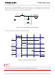

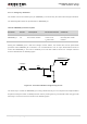

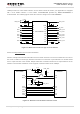
Table Of Contents
- About the Document
- Contents
- Table Index
- Figure Index
- 1 Introduction
- 2 Product Concept
- 3 Application Interface
- 3.1. General Description
- 3.2. Pin Assignment
- 3.3. Pin Description
- 3.4. Operating Modes
- 3.5. Power Saving
- 3.6. Power Supply
- 3.7. Turn on and off Scenarios
- 3.8. Reset the Module
- 3.9. RTC Interface
- 3.10. UART Interface
- 3.11. USIM Card Interface
- 3.12. USB Interface
- 3.13. PCM and I2C Interface
- 3.14. Network Status Indication
- 3.15. Operating Status Indication
- 4 Antenna Interface
- 5 Electrical, Reliability and Radio Characteristics
- 6 Mechanical Dimensions
- 7 Storage and Manufacturing
- 8 Appendix A Reference
- 9 Appendix B GPRS Coding Scheme
- 10 Appendix C GPRS Multi-slot Class
- 11 Appendix D EDGE Modulation and Coding Scheme

UMTS/HSPA Module Series
UG96 Hardware Design
UG96_Hardware_Design Confidential / Released 39 / 75
UG96 provides one 1.8V UART interface. A level shifter should be used if your application is equipped
with a 3.3V UART interface. A level shifter TXS0108EPWR provided by Texas Instruments is
recommended. The following figure shows the reference design of the TXS0108EPWR.
VCCA VCCB
OE
A1
A2
A3
A4
A5
A6
A7
A8
GND
B1
B2
B3
B4
B5
B6
B7
B8
VDD_EXT
RI
DCD
RTS
RXD
DTR
CTS
TXD
51K
51K
0.1uF
0.1uF
RI_3.3V
DCD_3.3V
RTS_3.3V
RXD_3.3V
DTR_3.3V
CTS_3.3V
TXD_3.3V
VDD_3.3V
TXS0108EPWR
10K
120K
Figure 20: Reference Circuit of Logic Level Translator
Please visit http://www.ti.com for more information.
Another example with transistor translation circuit is shown as below. The circuit of dotted line can refer to
the circuit of solid line. Please pay attention to direction of connection. Input dotted line of module should
refer to input solid line of the module. Output dotted line of module should refer to output solid line of the
module. The transistor translation circuit supports a maximum data rate of 0.5Mbps.
MCU/ARM
/TXD
/RXD
VDD_EXT
4.7K
VCC_MCU
4.7K
4.7K
VDD_EXT
TXD
RXD
RTS
CTS
DTR
RI
/RTS
/CTS
GND
GPIO DCD
Module
GPIO
EINT
VDD_EXT
4.7K
GND
1nF
1nF
Figure 21: Reference Circuit with Transistor Circuit