
User's Manual
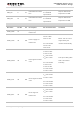
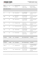
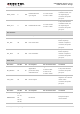
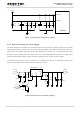
Table Of Contents
- About the Document
- Contents
- Table Index
- Figure Index
- 1 Introduction
- 2 Product Concept
- 3 Application Interface
- 3.1. General Description
- 3.2. Pin Assignment
- 3.3. Pin Description
- 3.4. Operating Modes
- 3.5. Power Saving
- 3.6. Power Supply
- 3.7. Turn on and off Scenarios
- 3.8. Reset the Module
- 3.9. RTC Interface
- 3.10. UART Interface
- 3.11. USIM Card Interface
- 3.12. USB Interface
- 3.13. PCM and I2C Interface
- 3.14. Network Status Indication
- 3.15. Operating Status Indication
- 4 Antenna Interface
- 5 Electrical, Reliability and Radio Characteristics
- 6 Mechanical Dimensions
- 7 Storage and Manufacturing
- 8 Appendix A Reference
- 9 Appendix B GPRS Coding Scheme
- 10 Appendix C GPRS Multi-slot Class
- 11 Appendix D EDGE Modulation and Coding Scheme

UMTS/HSPA Module Series
UG96 Hardware Design
UG96_Hardware_Design Confidential / Released 20 / 75
USB_DP
9
IO
USB differential data
bus.
Compliant with USB
2.0 standard
specification.
Require differential
impedance of 90Ω.
USB_DM
10
IO
USB differential data
bus.
Compliant with USB
2.0 standard
specification.
Require differential
impedance of 90Ω.
USIM Interface
Pin Name
Pin No.
I/O
Description
DC Characteristics
Comment
USIM_GND
47
Specified ground for
USIM card.
USIM_VDD
43
PO
Power supply for
USIM card.
For 1.8V USIM:
Vmax=1.85V
Vmin=1.75V
For 3.0V USIM:
Vmax=2.9V
Vmin=2.8V
Either 1.8V or 3.0V is
supported by the
module automatically.
USIM_DATA
45
IO
Data signal of USIM
card.
For 1.8V USIM:
V
IL
max=0.35V
V
IH
min=1.25V
V
OL
max=0.25V
V
OH
min=1.25V
For 3.0V USIM:
V
IL
max=0.5V
V
IH
min=2.05V
V
OL
max=0.25V
V
OH
min=2.05V
Pull-up to USIM_VDD
with 4.7K resistor
internally.
USIM_CLK
46
DO
Clock signal of USIM
card.
For 1.8V USIM:
V
OL
max=0.25V
V
OH
min=1.25V
For 3.0V USIM:
V
OL
max=0.25V
V
OH
min=2.05V
USIM_RST
44
DO
Reset signal of
USIM card.
For 1.8V USIM:
V
OL
max=0.25V
V
OH
min=1.25V
For 3.0V USIM:
V
OL
max=0.3V
V
OH
min=2.05V