
User's Manual

UMTS/HSPA Module Series
UG95 Hardware Design
UG95_Hardware_Design Confidential / Released 43 / 67
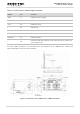
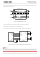
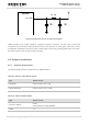
1. UG95 module can only be used as a slave device.
2. It is suggested to set USB_DP, USB_DM and USB_VBUS pins as test points and then place these
test points on the DTE for debug.
3. USB interface supports software debug and firmware upgrade by default.
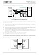
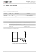
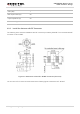
3.13. PCM and I2C Interface
UG95 provides one Pulse Code Modulation (PCM) digital interface for audio design, which supports the
following features:
Supports 8, 16, 32 bit mode with short frame synchronization, the PCM support 8 bit mode by default
since the PCM codec default configuration is AT+QDAI=1. Refer to document [1] for more details.
Supports master mode.
Supports audio sample rate 8 kHz.
The following table shows the pin definition of PCM and I2C interface which can be applied on audio
codec design.
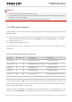
Table 16: Pin Definition of PCM and I2C Interface
Pin Name
Pin No. I/O
Description
Comment
PCM_CLK
4
IO
PCM data bit clock.
1.8V power domain.
PCM_SYNC
5
IO
PCM data frame sync signal.
1.8V power domain.
PCM_IN
6
DI
PCM data input.
1.8V power domain.
PCM_OUT
7
DO
PCM data output.
1.8V power domain.
I2C_SCL
40
DO
I2C serial clock.
Require external pull-up resistor.
I2C_SDA
41
IO
I2C serial data.
Require external pull-up resistor.
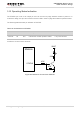
In PCM audio format the MSB of the channel included in the frame (PCM_SYNC) is clocked on the
second CLK falling edge after the PCM_SYNC pulse rising edge. The period of the PCM_SYNC signal
(frame) lasts for Data word bit +1 clock pulses.
UG95’s firmware has integrated the configuration on ALC5616 application with I2C interface. You can
execute command AT+QDAI=3 to configure the ALC5616 codec, and refer to document [1] for more
NOTE