
User's Manual

UMTS/HSPA Module Series
UG95 Hardware Design
UG95_Hardware_Design Confidential / Released 35 / 67
The logic levels are described in the following table.
Table 11: Logic Levels of Digital I/O
Parameter
Min.
Max.
Unit
V
IL
-0.3
0.35
V
V
IH
1.3
1.85
V
V
OL
0
0.25
V
V
OH
1.55
1.8
V
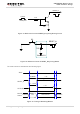
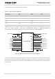
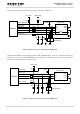
UG95 provides one 1.8V UART interface. A level shifter should be used if your application is equipped
with a 3.3V UART interface. A level shifter TXS0108EPWR provided by Texas Instruments is
recommended. The following figure shows the reference design of the TXS0108EPWR.
VCCA VCCB
OE
A1
A2
A3
A4
A5
A6
A7
A8
GND
B1
B2
B3
B4
B5
B6
B7
B8
VDD_EXT
RI
DCD
RTS
RXD
DTR
CTS
TXD
51K
51K
0.1uF
0.1uF
RI_3.3V
DCD_3.3V
RTS_3.3V
RXD_3.3V
DTR_3.3V
CTS_3.3V
TXD_3.3V
VDD_3.3V
TXS0108EPWR
Figure 17: Reference Circuit of Logic Level Translator
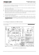
The reference design of 5V level match is shown as below. The construction of dotted line can refer to the
construction of solid line. Please pay attention to direction of connection. Input dotted line of module
should refer to input solid line of the module. Output dotted line of module should refer to output solid line
of the module.