
User's Manual

UMTS/HSPA Module Series
UG95 Hardware Design
UG95_Hardware_Design Confidential / Released 24 / 67
3.6. Power Supply
3.6.1. Power Supply Pins
UG95 provides four VBAT pins dedicated to connect with the external power supply. There are two
separate voltage domains for VBAT.
VBAT_RF with two pads for module RF.
VBAT_BB with two pads for module baseband.
The following table shows the VBAT pins and ground pins.
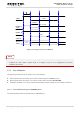
Table 6: VBAT and GND Pins
Pin Name
Pin No.
Description
Min.
Typ.
Max.
Unit
VBAT_RF
52,53
Power supply for module RF
part.
3.4
3.8
4.3
V
VBAT_BB
32,33
Power supply for module
baseband part.
3.4
3.8
4.3
V
GND
3,31,48,50
54,55,58,
59,61,62,
67~74,
79~82,
89~91,
100~102
Ground
-
-
-
-
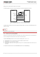
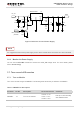
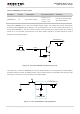
3.6.2. Decrease Voltage Drop
The power supply range of the module is 3.4V~ 4.3V. Because of the voltage drop during the transmitting
time, a bypass capacitor of about 100µF with low ESR should be used. Multi-layer ceramic chip (MLCC)
capacitor can provide the best combination of low ESR. Three ceramic capacitors (100nF, 33pF, 10pF)
are recommended to be applied to the VBAT pins. The capacitors should be placed close to the UG95’s
VBAT pins. The following figure shows star structure of the power supply.
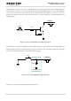
The main power supply from an external application has to be a single voltage source and has to be
expanded to two sub paths with star structure. In addition, in order to get a stable power source, it is
suggested to use a zener diode of whose reverse zener voltage is 5.1V and dissipation power is more
than 0.5W.