
User's Manual

UMTS/HSPA Module Series
UG95 Hardware Design
UG95_Hardware_Design Confidential / Released 20 / 67
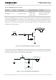
PCM_CLK
4
IO
PCM data bit clock.
V
OL
max = 0.25V
V
OH
min = 1.55V
V
IL
min = -0.3V
V
IL
max = 0.35V
V
IH
min = 1.3V
V
IH
max = 1.85V
1.8V power domain.
In master mode, it’s
an output signal.
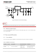
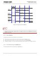
I2C Interface
Pin Name
Pin No.
I/O
Description
DC Characteristics
Comment
I2C_SCL
40
DO
I2C serial clock.
V
OL
max = 0.25V
V
OH
min = 1.55V
1.8V power domain.
External pull-up
resistor is required.
I2C_SDA
41
IO
I2C serial data.
V
OL
max = 0.25V
V
OH
min = 1.55V
V
IL
min = -0.3V
V
IL
max = 0.35V
V
IH
min = 1.3V
V
IH
max = 1.85V
1.8V power domain.
External pull-up
resistor is required.
Other Pins
Pin Name
Pin No.
I/O
Description
DC Characteristics
Comment
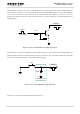
AP_READY
19
DI
Application
processor sleep
state detection.
V
IL
min = -0.3V
V
IL
max = 0.35V
V
IH
min = 1.3V
V
IH
max = 1.85V
1.8V power domain.
RESERVED Pins
Pin Name
Pin No.
I/O
Description
DC Characteristics
Comment
RESERV
ED
1,2,
11~14,18
22~28,
49,56,57,
63~66,
75~78,
83~88,
92~99.
Reserved
Keep these pins
unconnected.
AP_READY is under development.
NOTE