
User's Manual

UMTS/HSPA Module Series
UG95 Hardware Design
UG95_Hardware_Design Confidential / Released 16 / 67
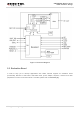
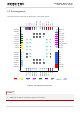
3.3. Pin Description
The following tables show the UG95’s pin definition.
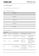
Table 3: IO Parameters Definition
Type
Description
IO
Bidirectional input/output
DI
Digital input
DO
Digital output
PI
Power input
PO
Power output
AI
Analog input
AO
Analog output
OD
Open drain
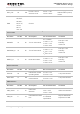
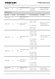
Table 4: Pin Description
Power Supply
Pin Name
Pin No.
I/O
Description
DC Characteristics
Comment
VBAT_BB
32,33
PI
Power supply for
module baseband
part.
Vmax = 4.3V
Vmin = 3.4V
Vnorm = 3.8V
It must be able to
provide sufficient
current up to 0.8A.
VBAT_RF
52,53
PI
Power supply for
module RF part.
Vmax = 4.3V
Vmin = 3.4V
Vnorm = 3.8V
It must be able to
provide sufficient
current in a transmitting
burst which typically
rises to 2.0A.
VRTC
51
PI/
PO
Power supply for
internal RTC circuit.
V
O
max = 1.9V
when VBAT ≥ 3.4V.
V
I
= 1V~1.9V at
I
IN
max = 2uA when
VBAT is not applied.
Keep this pin
unconnected if unused.