
User Manual

UMTS/HSDPA Module Series
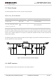
UC15 Mini PCIe Hardware Design
UC15_Mini_PCIe_Hardware_Design Confidential / Released 15 / 40
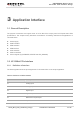
Table 4: Description of Pin
PI Power input
PO Power output
Pin No.
Mini PCI Express
Standard Name
UC15 Mini PCIe
Name
I/O Description Comment
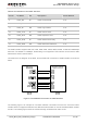
1 WAKE# MICP* AI
Audio positive input
2 3.3Vaux VCC_3V3 PI 3.3V DC supply
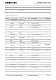
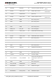
3 COEX1 MICN* AI Audio negative input
4 GND GND — Mini card ground
5 COEX2 SPKP* AO Audio positive output
6 1.5V NC — —
7 CLKREQ# SPKN* AO Audio negative output
8 UIM_PWR USIM_VDD PO
Power source for the USIM
card
9 GND GND — Mini card ground
10 UIM_DATA USIM_DATA IO USIM data signal
11 REFCLK- UART_RX DI UART receives data
Connect to
DTE’s TX.
12 UIM_CLK USIM_CLK DO USIM clock signal
13 REFCLK+ UART_TX DO UART transmits data
Connect to
DTE’s RX.
14 UIM_RESET USIM_RST DO USIM reset signal
15 GND GND — Mini card ground
16 UIM_VPP RESERVED — Reserved
17 RESERVED UART_RI DO UART ring indicator
18 GND GND — Mini card ground
19 RESERVED RESERVED — Reserved
20 W_DISABLE# W_DISABLE# DI
Disable wireless
communications
Active low.
21 GND GND
— Mini card ground