
User's Manual

UMTS/HSDPA Module Series
UC15 Hardware Design
UC15_Hardware_Design Confidential / Released 47 / 78
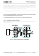
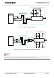
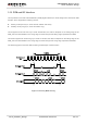
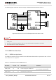
Figure 28: Auxiliary Mode Timing
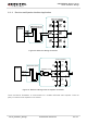
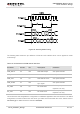
The following table shows the pin definition of PCM and I2C interface which can be applied on audio
codec design.
Table 16: Pin Definition of PCM and I2C Interface
UC15’s firmware has integrated the configuration on NAU8814 application with I2C interface. The default
configuration is master mode which uses short sync data format with 2048 kHz clock. Please refer to
document [1] for details about the command AT+QDAI.
Pin Name Pin No. I/O Description Comment
PCM_DOUT 34 DO PCM data output. 2.6V power domain
PCM_DIN 35 DI PCM data input. 2.6V power domain
PCM_CLK 36 IO PCM data bit clock. 2.6V power domain
PCM_SYNC 37 DO
PCM data frame
sync signal
2.6V power domain
I2C_SDA 38 IO I2C serial data.
External pull-up resistor is
required. 2.6V only.
I2C_SCL 39 DO I2C serial clock.
External pull-up resistor is
required. 2.6V only.