
User's Manual

UMTS/HSDPA Module Series
UC15 Hardware Design
UC15_Hardware_Design Confidential / Released 19 / 78
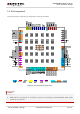
3.3. Pin Description
The pin definition of UC15 is shown in table 4.
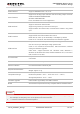
Table 3: IO Parameters Definition
Table 4: Pin Description
Type Description
IO Bidirectional input/output
DI Digital input
DO Digital output
PI Power input
PO Power output
AI Analog input
AO Analog output
Power Supply
Pin Name Pin No. I/O Description DC Characteristics Comment
VBAT_BB 52,53 PI
Power supply for
module baseband
part.
Vmax=4.3V
Vmin=3.3V
Vnorm=3.8V
It must be able to
provide sufficient
current up to 0.8A.
VBAT_RF 50,51 PI
Power supply for
module RF part.
Vmax=4.3V
Vmin=3.3V
Vnorm=3.8V
It must be able to
provide sufficient
current in a
transmitting burst
which typically
rises to 2.0A.
VDD_EXT 7 PO
Provide 2.6V for
external circuit.
Vnorm=2.6V
I
O
max=100mA
It is recommend to
add a 2.2~4.7uF
bypass capacitor
when using this
pin for power
supply.