
User Manual


GSM/GPRS Module Series
GC10 Hardware Design
GC10_Hardware_Design Confidential / Released 23 / 76
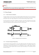
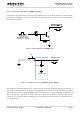
The VBAT route should be wide enough to ensure that there is not too much voltage drop during transmit
burst. The width of trace should be no less than 2mm and the principle of the VBAT route is the longer
route, the wider trace.
Figure 4: Reference Circuit for the VBAT Input
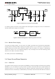
3.3.3. Reference Design for Power Supply
The power design for the module is very important, since the performance of power supply for the module
largely depends on the power source. The power supply is capable of providing the sufficient current to
2A at least. If the voltage drop between the input and output is not too high, it is suggested to use a LDO
as module’s power supply. If there is a big voltage difference between the input source and the desired
output (VBAT), a switching power converter is recommended to be used as a power supply.
Figure 5 shows a reference design for +5V input power source. The designed output for the power supply
is 4.16V and the maximum load current is 3A. In addition, in order to get a stable output voltage, a zener
diode is placed close to the pins of VBAT. As to the zener diode, it is suggested to use a zener diode
whose reverse zener voltage is 5.1V and dissipation power is more than 1 Watt.