
User Manual


GSM/GPRS Module Series
GC10 Hardware Design
GC10_Hardware_Design Confidential / Released 22 / 76
Use the EMERG_OFF pin only when failing to turn off the module by the command “AT+QPOWD=1” and
the PWRKEY pin. For more details, please refer to Section 3.4.2.4.
3.3. Power Supply
3.3.1. Power Features of Module
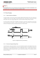
The power supply is one of the key issues in designing GSM terminals. Because of the 577us radio burst
in GSM every 4.615 ms, power supply must be able to deliver high current peaks in a burst period. During
these peaks, drops on the supply voltage must not exceed minimum working voltage of module.
For GC10 module, the max current consumption could reach to 1.6A during a transmit burst. It will cause
a large voltage drop on the VBAT. In order to ensure stable operation of the module, it is recommended
that the max voltage drop during the transmit burst does not exceed 400mV.
Figure 3: Voltage Drop during Transmitting
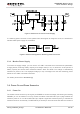
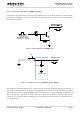
3.3.2. Decrease Supply Voltage Drop
The power supply range of the module is 3.3V to 4.6V. Make sure that the input voltage will never drop
below 3.3V even in a transmitting burst. If the power voltage drops below 3.3V, the module could turn off
automatically. For better power performance, it is recommended to place a 1000uF tantalum capacitor
with low ESR and ceramic capacitor 100nF, 47pF and 10pF near the VBAT pin. The reference circuit is
illustrated in Figure 4.
NOTE