
User Manual


GSM/GPRS Module Series
GC10 Hardware Design
GC10_Hardware_Design Confidential / Released 20 / 76
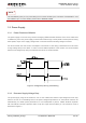
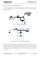
SIM_RST 24 O SIM reset
array. Maximum trace
length is 100mm from
the module pad to SIM
card holder.
SIM_ DATA 25 I/O
SIM data
SIM_CLK 26 O SIM clock
SIM_GND 27 SIM ground
SIM_
PRESENCE
28
I
SIM card detection
VILmin=0V
VILmax=
0.3×VDD_EXT
VIHmin=
0.7×VDD_EXT
VIHmax=
VDD_EXT
SIM_PRESENCE
must be pulled up by
an external resistor
when SIM card
detection function is
used.
PCM Interface
Pin Name
Pin
NO.
I/O
Description DC Characteristics Comment
PCM_ IN 1 I PCM data input
VILmin=0V
VILmax=
0.3×VDD_EXT
VIHmin=
0.7×VDD_EXT
VIHmax=
VDD_EXT
VOLmin=0V
VOLmax=
0.3×VDD_EXT
VOHmin=
0.7×VDD_EXT
VOHmax=
VDD_EXT
PCM function is not
supported at present.
If unused, keep these
pins open.
PCM_SYNC
2
O
PCM frame
synchronization
PCM_ OUT 3 O PCM data output
PCM_ CLK 4 O PCM clock
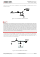
RF Interface
Pin Name
Pin
NO.
I/O
Description DC Characteristics Comment
RF_ANT 38 I/O
RF antenna pad Impedance of 50Ω
Please refer to
Chapter 4
Other Interface
Pin Name
Pin
NO.
I/O
Description DC Characteristics Comment
RESERVED
41,42,
43,44
Please keep these
pins open.